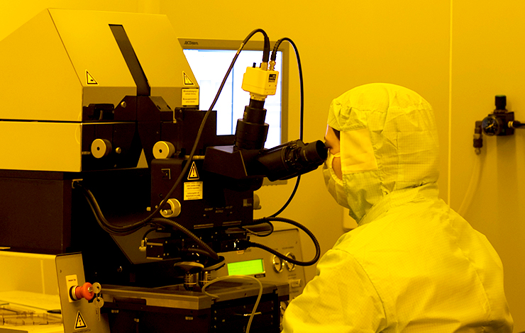


Clean Room (Production) Lab
Luís Pereira (ext. 13753)
Description:
The thin-film deposition area is an ISO 7 lab devoted to the preparation of thin films by physical and chemical vapor deposition techniques, as required to fabricate micro/nanoscale devices.
The lab is equipped with a wide range of physical and chemical vapor deposition tools to fabricate a variety of thin film materials, such as metals, (transparent) conductors and semiconductors and insulators, with nm-thickness control. Most systems can accommodate up to 6” wafers. Tools include 5 sputtering, 2 plasma-enhanced chemical vapor deposition (PECVD), 4 evaporation and 1 CVD (parylene coater) systems. A rapid thermal processing (RTP) tool is also available for post-deposition treatments of thin films. A plasma-enhanced atomic layer deposition (PEALD) system with a glovebox for substrate loading/unloading in controlled environment will be installed in July 2019.


