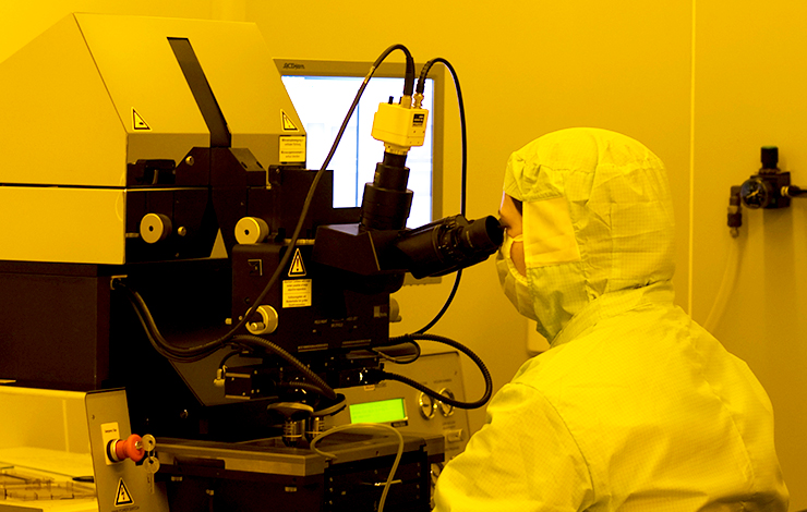


X-ray and Ultraviolet Photoelectron Spectroscopy (XPS/UPS)
Responsible: Jonas Deuermeier
Description:
Photoelectron spectroscopy is a surface analysis tool for chemical and electronic characterization of materials. Its distinguishing feature is the possibility to measure chemical states. The information depth is 1-9 nm. The technique relies on the photoelectric effect. The photoexcitation energies typically range from ~20 eV (UPS) to ~1.5 keV (XPS). The photoelectrons are filtered regarding their kinetic energy by the analyzer and counted by the detector. The lower the kinetic energy of the photoelectron, the more tightly it was bound to the nucleus, so the higher is its binding energy. Besides chemical information, also electrostatic potential at surfaces and interfaces can be studied.
Specifications:
• Excellent compromise between energy resolution and sensitivity:
0.44 eV at 200 kcps (XPS)
0.60 eV at 2 Mcps (XPS)
0.01 eV at 1 kcps (UPS)
• Lateral resolution for spectroscopy: 15 µm
• Imaging capability with lateral resolution of 1 µm and infinite size (by image stitching)
• Rapid “snapshot” spectroscopy
• Angle-resolved measurement and azimuthal rotation
• Pressure in analysis chamber down to 5e-10 Torr
• Sample holder size 9 x 3 cm
Main features and Accessories:
• 165 mm mean radius hemispherical and spherical mirror analyzer
• Delay-line detector
• Magnetic immersion lense
• Electron-only charge neutralization
• Monochromatic Al source (1486.6 eV)
• Argon cluster sputter gun (up to 2000 atoms)
• Heating and cooling in load-lock and analysis chamber (-120°C to 800°C)
• Helium discharge lamp for UPS (He I: 21.22 eV, He II: 40.8 eV)
• Ion scattering spectrometry (ISS)
• Dual achromatic source (Al/Mg)
• Sample transfer chamber for transport of air-sensitive samples


