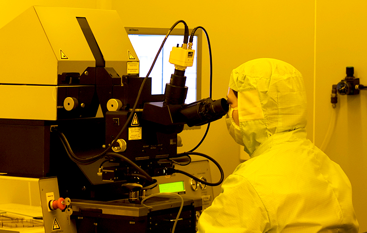


Laboratory of Electronic and Optoelectronic Materials and Devices

I- Production/Processes
Here we have 3 main areas which are:
a) >104 clean classroom with the following facilities: 7 rf magnetron sputtering (one able to process 30 cm × 40 cm area and another with a load-lock); 4 electron gun systems; a spray pyrolysis and a deep coater, all devoted to the production and development of single and multicomponent, undoped and doped oxide semiconductors and high-k dielectrics (simple and multi-structures) such as zinc, tin, zirconium, molybdenum, tungsten vanadium, hafnium, titanium and other composite oxides for different optoelectronic and electronic applications. This area also includes 5 plasma enhanced chemical vapour deposition PECVD, (2 semi-industrials); one hot wire plasma assisted deposition systems, able to process amorphous, nanocrystalline and polycrystalline silicon based materials and devices. The laboratory also has 2 thermal evaporators and an electrodeposition unit for processing metal contacts and joins and atmosphere control furnaces for materials/device treatments.
b) <104 clean classroom with two microwelding systems (wave and dye bond); a double beam YAG laser for scribing films or processing masks with resolutions up to 20 m; a laminator for packaging/encapsulating devices; a dicing saw; and a mechanical scriber.
c) < 103 classroom with 6 automated diffusion furnaces; a LPCVD unit for processing polycrystalline silicon; a dry etching with an end point detector; 3 spinners; a manual and a semi-automatic mask aligner; cleaners; developers and etchers; profilometers and an ellipsometer.
II- Characterization
This laboratory is equipped with a wide range of techniques such as: infrared and visible spectroscopy’s; 2 quantum efficiency (spectral response) systems; 4 solar simulators; PDS and CPM; spectroscopic ellipsometry; FTIR; 3 cryostat units to measure the electrical and optical properties of materials/devices as a function of temperature; DLTS; Hall effect; 2 four probe units to measure the sheet resistance; exodifusion unit; profilometers; in-situ recrystallization unit; gas sensor test unit; C-V system; 2 semiconductor analyser; two microprobe unit station; two wide range microscopes; time transient measurement unit.
III- Equipments


