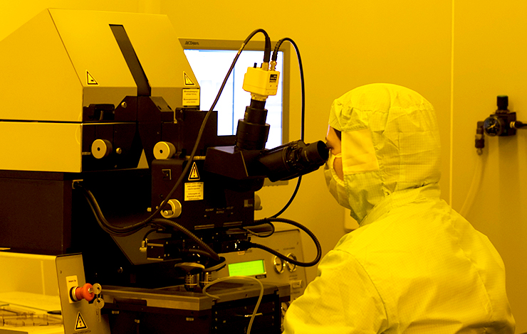


Materials for Electronics, Optoelectronics and Nanotechnologies (MEON)
The Materials for Electronics, Optoelectronics and Nanotechnologies (MEON) group has a strong activity in fab (e.g. PECVD, PVD, sol gel, spray pyrolysis) and non fab processes (e.g. inkjet) with strong experience in the development of materials for key enabling technologies. Here emphasis is put in exploiting materials’ outstanding performances at a nanoscale, almost by design, for electronics and optoelectronic industry (Samsung, Suzano, Saint Gobain), pioneering international research on full oxide TFT as well as on paper electronics (Paper-e®).
The group is considered one of the world pioneers in the so-called transparent electronics, being the inventors of the oxide transparent thin film transistors processed at room temperature and was one of the first world group proving the superiority in using amorphous oxide films either for passive applications such as transparent conductive oxides or active semiconductors, such as the channel layer in field effect based transistors. They coordinated the first project of active oxides (Multiflexioxides), considered by the EU as one of the 10 outstanding projects within FP6.


