


OFERTA FORMATIVA DCM - FCT/UNL
Navigation
Recyclable circuits – easy on paper Complementary metal oxide semiconductor technology using paper

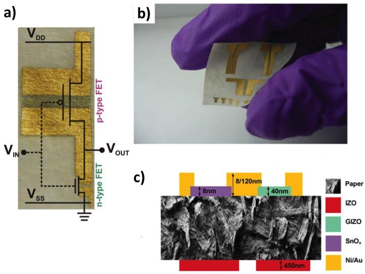
Complementary metal oxide semiconductor (CMOS) circuit based on n-type (In-Ga-Zn-O) and p-type (SnOx) metal-oxide semiconductors that sits on a flexible, recyclable paper substrate.
Today’s electronics demand portable, flexible, low cost and easily recyclable devices. In addition, these should have low power consumption, to be adopted in a plethora of circuits ranging from computer memory, digital logic and microprocessors, to (linear) analogue circuits. Paper is the lightest, most flexible, robust and cheap material that is fully recyclable.
A team of researchers from Universidade Nova de Liboa (Caparica, Portugal) and the London Centre for Nanotechnology (UCL, London, UK) have demonstrated a working, low-power CMOS inverter on a flexible, recyclable, fiber-based paper substrate. This major breakthrough was made possible following the advent of both n-type and p-type metal-oxide semiconductors, which are the fundamental building blocks of digital logic. Paper, which serves as a gate dielectric, enhances the transistor’s transconductance due to a large dielectric capacitance at lower frequencies, a virtue of its fibrous foam-like structure. The result of this advance is published in Advanced Materials this week.
“The inverter has a low static power consumption and well defined voltage transfer characteristic with a sharp state transition making its useful as a building block of digital circuits thus creating an opportunity for light weight, low cost and fully recyclable complimentary CMOS circuits” says Prof. Arokia Nathan, the principal investigator at the LCN.
Prof Rodrigo Martins, the lead author of this paper concludes that this is expected to create applications in disposable, recyclable electronics that range from smart labels, tags, sensors and memories to thin film transistor driven electrochromic paper displays and integrated systems.
For full paper please visit:
http://dx.doi.org/10.1002/adma.201102232
Figure:
a) Microphotograph of the CMOS on paper where the large and small device areas correspond to the p-FET and n-FET, respectively.
b) Image of the circuit showing its flexibility.
c) Cross-sectional schematic of the paper CMOS circuit showing all layers that constitute the final devices and their interconnection.